
Finland's microelectronics and quantum technology RDI cluster and cleanroom environment
What is Kvanttinova?
Kvanttinova comprises three entities:
- Kvanttinova Ltd.: The company that builds the ecosystem of microelectronics and quantum players in Espoo, Finland.
- Kvanttinova ecosystem: The community of companies that are members of and using the facilities in the Micronova and Kvanttinova buildings.
- Kvanttinova Hub: The new building next to Micronova that will offer new cleanroom facilities.
Kvanttinova Ltd.: Helping microelectronics and quantum players access the Kvanttinova ecosystem in Espoo, Finland
Kvanttinova Ltd. helps startups, companies, investors, and scientists build real-world impact in Espoo's Kvanttinova ecosystem in microelectronics, photonics and quantum technologies. Kvanttinova Ltd. builds a collaborative ecosystem so the players can access the ecosystem's piloting facilities, learning opportunities, and scaling capabilities in the best way possible — helping innovators in chips and chip-based systems to move faster and grow their business together.
Go to Kvanttinova Ltd. web page
Kvanttinova ecosystem: A high-profile European chip innovation ecosystem
The Kvanttinova ecosystem brings together deep tech startups, scaleups, small, medium-sized, and large companies, as well as academia and technology organisations in the fields of quantum technologies, microelectronics, and photonics. The Kvanttinova ecosystem focuses on advanced microelectronics technologies, such as MEMS, integrated photonics, CMOS, post-CMOS, RF, and quantum technologies.
The ecosystem is built on collaboration. Experts and educators can work with members, partners and friends in the local Otaniemi district, Espoo, and the Helsinki metropolitan area. The Kvanttinova ecosystem's players are key drivers for the semiconductor industry's growth in Finland and Europe.
The Kvanttinova ecosystem utilises VTT's open access microelectronics technology infrastructure in Micronova and Aalto University's open access microelectronics research infrastructure OtaNano. Companies can use the shared facilities for research, development, and production. The Kvanttinova ecosystem includes players with world-leading quantum tech expertise, especially in superconducting quantum technologies, with activities including material development and concept innovation to circuit design, fabrication, prototyping, piloting, and production.
Kvanttinova hub: A building offering more cleanroom space next to Micronova
The Kvanttinova hub will be a new building next to Micronova, the largest cleanroom in the Nordics. Micronova is the location for VTT and Aalto University's cleanroom spaces. The Kvanttinova building will offer more cleanroom space for companies and VTT. VTT will facilitate the new cleanroom in the coming Kvanttinova hub.
Why cooperate?
Kvanttinova strengthens Finland's position as one of Europe's most important microelectronics and quantum technology hubs. The European Union and the United States Chip Acts aim to decrease dependencies on global value chains originating elsewhere. The European Chips Act seeks to double the European market share to 20% by 2030. This requires both new deep technology investments and increased manufacturing capacity. Kvanttinova contributes to the European technological leadership on chips. Kvanttinova serves these specialised microelectronics processes in a highly integrated fashion.
Currently, most of the world's microchips are manufactured using CMOS technology. However, Finland is a pioneer in specialised microelectronics processes such as integrated photonics, MEMS sensors, radio frequency communications, silicon-based detectors and quantum technology. The added value of these technologies comes from entirely new functionalities that cannot be implemented with CMOS technology.
The purpose of Kvanttinova is to increase the sector's RDI activities in Finland, boost product and service exports, and attract new international experts, companies and investments.
Who runs Kvanttinova?
Kvanttinova is a joint initiative by VTT Technical Research Centre of Finland, the City of Espoo, Aalto University and the industry members of the semiconductor industry group of Technology Industries of Finland. Requirements for the buildings and equipment are being collected from the industry to enable future growth and quadruple both the number of employees and revenues by 2032.
Kvanttinova is a part of the "Chips from the North" initiative.


Want to know more about Kvanttinova?


Miska
Hakala

Ossi
Ritvos
Micronova
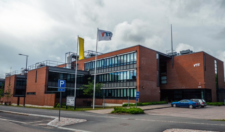
Kvanttinova expands the already existing research infrastructure Micronova, located in Espoo. Micronova features two cleanrooms, with processing capabilities for silicon-based CMOS, MEMS and photonics devices, 3D integration and thin film components.
Micronova offers cleanroom services and the entire development cycle of micro- and nanofabrication from fundamental research to small-scale production.
Related content

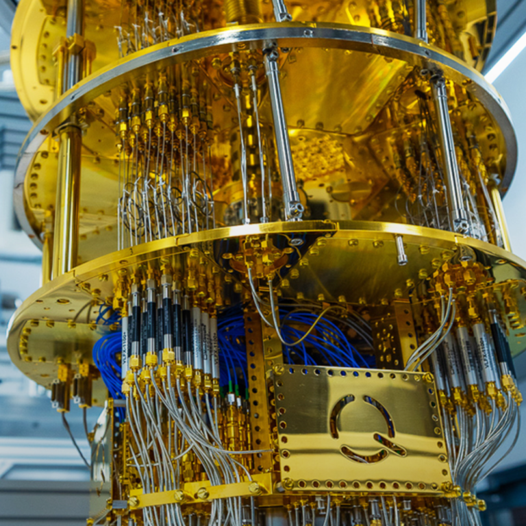

Image: VTT